(China (Mainland))

Product Summary
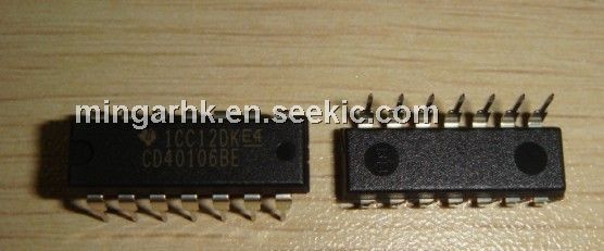
CD40106B consists of sic Schmittrigger circuits.Each circuits functions as an inverter with Schmitt-trigger action on the input.
The trigger switches at different points for positive and negative-going signals.The difference between the positive-going
voltage (VP) and the negative-going voltage(VN) is defined as hysteresis voltage (VH).
Parametrics
Absolute Maximum Ratings:
- DC Supply-Voltage Range,Voltage referenced to Vss Terminal:-0.5V to +20V
- Input Voltage range,all inputs:-0.5V ro VDD+0.5V
- DC input current,any one input:±10mA
- Power dissipation per package,For TA=-55℃ to +100℃:500mW;For TA=+100℃ to +125℃:Derate Linearity at 12mW/℃ to 200mW
- Device dissipation per output transistor,For TA=Full package-temperature range(All package types):100mW
- Operation-temperature range:-55℃ to +125℃
- Storage temperature (During Soldering),at distance 1/16± 1/32inch(1.59±0.79mm) from case for 10s max:+265℃
Features
- Schmitt-trigger action with no external components
- Hysteresis voltage(typ) 0.9V at VDD=5V,2.3V at VDD=10V,and 3.5V at VDD=15V
- Noise immunity greater than 50%
- No limit on input rise and fall times
- Standardized,symmetrical output characteristics
- 100% tested for quiescent current at 20V
- Maximum input current of 1μA at 18V over full package-temperature range;100nA at 18V and 25℃
- Low VDD to Vss current during slow input ramp
- 5V,10V,and 15V parametric ratings
Diagrams

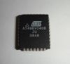
| Image | Part No | Mfg | Description |  |
Pricing (USD) |
Quantity | ||||||||||||
|---|---|---|---|---|---|---|---|---|---|---|---|---|---|---|---|---|---|---|
 |
 CD40106BE |
Texas Instruments |
Inverters Hex Schmitt Trigger |
Data Sheet |
|
|
||||||||||||
|
CD40106BEE4 |
Texas Instruments |
Inverters Hex Schmitt Trigger |
Data Sheet |
|
|
||||||||||||